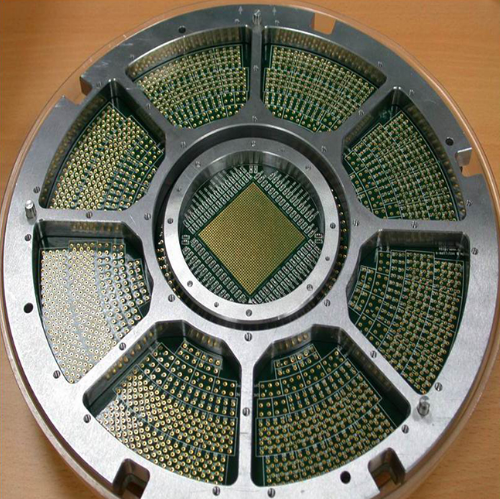
With the continuous advancement of the semiconductor industry, the dimensions of wafers and the spacing between bond pads have become increasingly smaller, presenting new challenges for wafer aging testing. To address these challenges, our wafer Burn in test fixture features an innovative micro-pitch probe card structure, specifically designed to meet these high-precision requirements, ensuring the effectiveness and reliability of the testing.
Superior Probe Card Structure The design of the micro-pitch probe card structure not only enhances the accuracy of testing but also significantly reduces the risk of short circuits and poor contact. This structure optimizes the shape and material of the probes, enabling precise contact within extremely small pad spacing. Stable electrical connections not only improve the reliability of aging tests but also ensure signal integrity during high-frequency signal testing.

- Handling Dimensional Tolerances There is a certain tolerance in the external dimensions of wafers, and traditional test fixtures often struggle to accommodate these variations. Our test fixture adopts a flexible design that can effectively handle wafers of different dimensions. The construction of the test fixture takes into account various tolerance factors, ensuring that each test maintains a high degree of consistency. This design not only improves production efficiency but also reduces testing errors caused by incompatibility. For example, if the wafer spacing is 0.125mm and the pad size is 0.07*0.07mm, it is clear that the spacing is too small, and the pad size is even smaller. There is also tolerance in the wafer size, which cannot be accommodated by conventional positioning. It requires the use of external microscope equipment for fine-tuning and alignment. After adjusting the contact, the cover is closed directly to complete the contact.
- Cooperation with Microscope Fine-Tuning Equipment To further enhance the testing accuracy of micro-pitch, our test fixture is equipped with advanced microscope fine-tuning equipment. Operators can observe the contact situation between the probe and the pad in real-time through the microscope and make precise adjustments at the microscopic level. This high-precision fine-tuning capability ensures that each testing link reaches the best state, ensuring the optimal contact between the probe and the pad, thereby greatly enhancing the flexibility and effectiveness of the testing.
- Aging / Burn in Tests Applicable to Wafer Socket
- High-Temperature Storage (HTS): Temperature condition: Usually conducted at around 150°C, with specific temperatures depending on the specifications and testing requirements of the device.
- High-Temperature Operating Life (HTOL): Temperature condition: Usually between 125°C and 150°C, with specific temperatures depending on the working conditions and testing standards of the device.
- High-Temperature Reverse Bias (HTRB): Temperature condition: Usually at around 150°C, while applying reverse bias.
- High-Temperature Accelerated Life Test (H-ALT): Temperature condition: Usually between 125°C and 150°C, with specific temperatures depending on the acceleration factor and the tolerance of the device.
- High-Temperature High-Humidity Bias (THB): Temperature condition: Usually between 85°C and 125°C, conducted in a high-humidity environment.
- Dynamic Thermal Cycling (DTC): Temperature condition: Involves cycling between high and low temperatures, with high temperatures usually around 125°C, and low temperatures depending on the specifications and testing requirements of the device.
- Mechanical Stress Testing: Temperature condition: This type of testing mainly focuses on mechanical stress but may be conducted at room temperature or specific temperatures to simulate actual usage conditions.
- Electromigration Testing: Temperature condition: Usually between 100°C and 150°C, with specific temperatures depending on the working conditions and testing standards of the device.
- Time Zero Failure Testing: Temperature condition: This type of testing may be conducted at room temperature or specific temperatures to assess the reliability of the device in its initial state.
- Highly Accelerated Stress Test (HAST): Temperature condition: Usually between 85°C and 130°C, conducted in a steam environment with 85% relative humidity.
The combination of ANDK’s micro-pitch probe card structure Socket and microscope fine-tuning equipment ensures that our wafer aging test fixture performs exceptionally in terms of testing accuracy and reliability. No matter how small the spacing, with the cooperation of these two devices, it can be properly placed into the aging chamber for electrical and reliability testing.
发表回复