1.Abstract:
HBM DRAM chip testing poses several challenges due to its small size, tight spacing, and unique testing requirements. This article discusses the difficulties encountered in testing HBM DRAM chips, including the need for specialized testing fixtures, high-speed testing, high-temperature aging, and precise microscopic alignment. The article highlights the importance of using microscopy for aligning the chip’s pins with the testing fixture, confirming multiple pin contacts, and securely closing the fixture to ensure reliable connections. Additionally, it emphasizes the significance of temperature and environmental control during high-temperature aging tests. Overall, this article provides insights into the complexities of testing HBM DRAM chips and the critical factors to consider for accurate and reliable testing results.
2.Keywords:
HBM DRAM, chip testing, small size, tight spacing, high-speed testing, high-temperature aging, microscopic alignment, HBM burn in test.

3. Introduction:
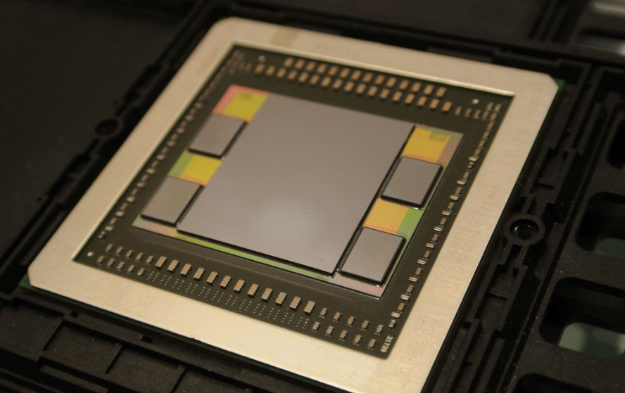
HBM (High Bandwidth Memory) DRAM chips are known for their small size and tight spacing, presenting unique challenges in the testing process. This article aims to explore the difficulties encountered in testing HBM DRAM chips and the specific requirements for successful testing. The challenges discussed include the need for specialized testing fixtures, high-speed testing capabilities, high-temperature aging tests, and precise microscopic alignment. Understanding these challenges is crucial for ensuring accurate and reliable testing results.
- Specialized Testing Fixtures: Due to the small size and tight spacing of HBM DRAM chips, conventional testing fixtures with limiting frames are inadequate for proper chip placement. Instead, specialized testing fixtures that allow for precise alignment and secure connections are required. Microscopy plays a vital role in this process, enabling operators to observe and adjust the chip’s position under magnification. This ensures that each pin makes perfect contact with the corresponding contact point on the testing fixture.
- High-Speed Testing: HBM DRAM chips often operate at high frequencies and data transfer speeds. Therefore, the testing process must support high-speed signal transmission and capture to accurately assess the chip’s performance. Specialized testing equipment capable of handling high-speed signals is necessary to ensure reliable testing results.
- High-Temperature Aging Tests: To validate the stability and reliability of HBM DRAM chips under high-temperature conditions, high-temperature aging tests are often conducted. This requires testing equipment that can operate reliably at elevated temperatures and accurately record and analyze the chip’s performance under such conditions. Temperature and environmental control are critical factors to consider during these tests to ensure consistent and accurate results.
- Microscopic Alignment: The microscopic structure and intricate layout of HBM DRAM chips necessitate precise access and testing of various functional modules within the chip. Microscopy is essential for aligning the chip’s pins with the testing fixture, ensuring optimal contact and reliable testing results. Operators must meticulously confirm the contact status of multiple pins to avoid testing failures caused by poor contact.
Conclusion:
Testing HBM DRAM chips presents unique challenges due to their small size, tight spacing, and specific testing requirements. Specialized testing fixtures, high-speed testing capabilities, high-temperature aging tests, and precise microscopic alignment are crucial factors to consider for accurate and reliable testing results. Understanding these challenges and implementing appropriate testing methodologies are essential for ensuring the quality and performance of HBM DRAM chips in various applications.
发表回复