Basic Structure:
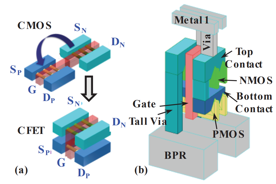
- Stacked Architecture: The CFET device adopts a vertical stacking approach, layering P-type and N-type FETs (Field-Effect Transistors) on top of each other. This architecture not only saves planar space but also effectively enhances transistor performance.
- Source/Drain Contacts: This design includes source/drain contacts at both the bottom and top, allowing each FET to operate independently without mutual interference.

Advantages:
- High-Density Integration: By vertically stacking P-type and N-type FETs, this design significantly increases the transistor density in integrated circuits.
- Performance Enhancement: CFET can better manage current paths and reduce parasitic capacitance, thereby improving overall performance.
- Power Optimization: The stacked structure helps reduce leakage current and dynamic power consumption, making the device more energy-efficient.
Basic Function: Logic Gate Circuits
CMOS CFET devices are commonly used to construct logic gate circuits, such as AND, OR, NOT, etc., which are fundamental components of digital circuits. Utilizing its high density and low power characteristics, CMOS CFET can achieve efficient logical operations and signal processing.
Advantages of ANDK Test Sockets with CMOS CFET Devices

The ANDK test socket pairs exceptionally well with CMOS CFET devices in logic gate circuit applications, as evidenced by the following aspects:
Precise Electrical Performance Testing:
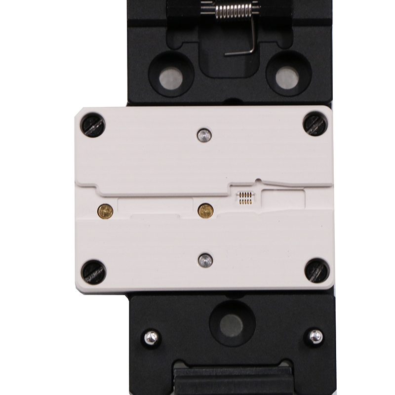
ANDK test sockets can accurately interface with the source/drain contacts of CFET devices for static and dynamic electrical performance testing. For logic gate circuits, key metrics include response speed, power consumption, and stability, which ANDK can effectively evaluate.
Low Power and High-Speed Verification:
CMOS CFET devices offer advantages such as low static power consumption and high-speed operation in logic gate circuits. ANDK test sockets can verify these advantages, ensuring the devices meet design requirements for power and speed in practical applications.
Thermal Characteristics Testing:
ANDK test sockets support thermal characteristic testing of CFET devices, which is crucial for high-density integrated circuits. The stability and thermal management capability of logic gate circuits under prolonged operation and high-frequency conditions are critical considerations.
High Throughput and Automated Testing:
For mass production and quality control, the high throughput and automation features of ANDK test sockets are particularly important. They can quickly and accurately test the performance of each CFET device, ensuring consistency and reliability of the overall product.
发表回复